
While we try to keep things accurate, this content is part of an ongoing experiment and may not always be reliable.
Please double-check important details — we’re not responsible for how the information is used.
Artificial Intelligence
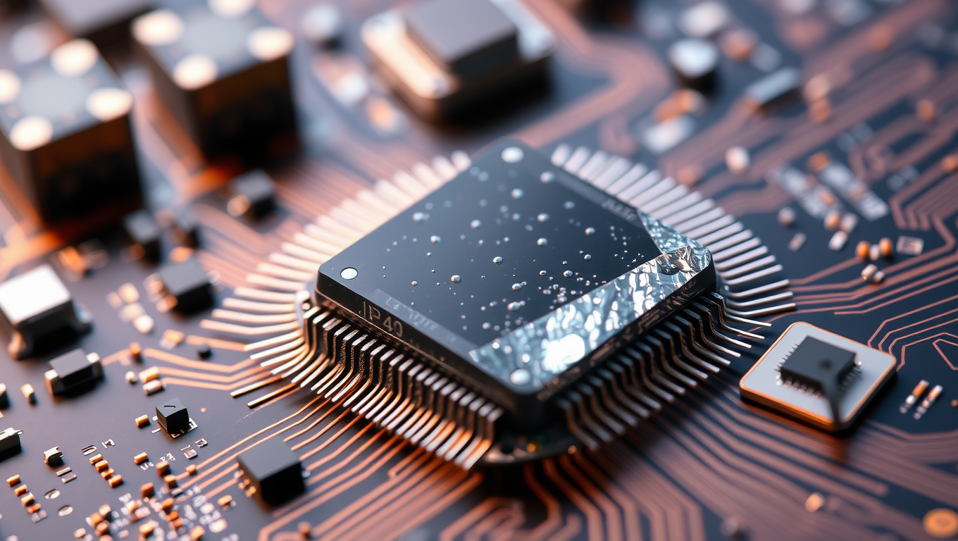
Transistors Get a Boost: Scientists Develop New, More Efficient Material
Shrinking silicon transistors have reached their physical limits, but a team from the University of Tokyo is rewriting the rules. They’ve created a cutting-edge transistor using gallium-doped indium oxide with a novel “gate-all-around” structure. By precisely engineering the material’s atomic structure, the new device achieves remarkable electron mobility and stability. This breakthrough could fuel faster, more reliable electronics powering future technologies from AI to big data systems.


Artificial Intelligence
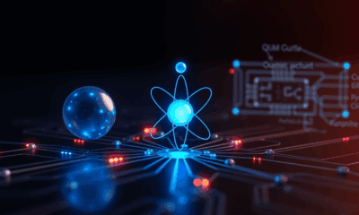
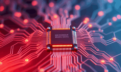
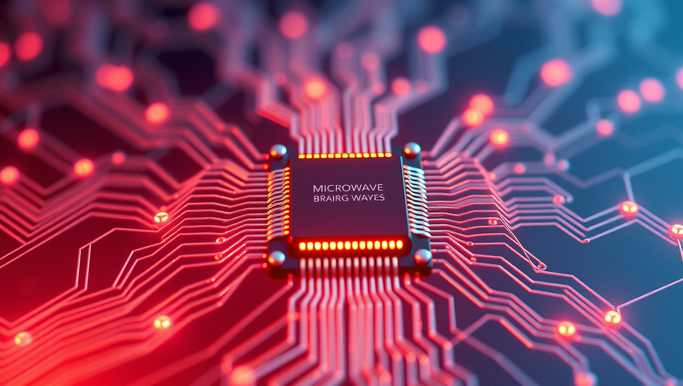
“Revolutionizing Computing with the ‘Microwave Brain’ Chip”
Cornell engineers have built the first fully integrated “microwave brain” — a silicon microchip that can process ultrafast data and wireless signals at the same time, while using less than 200 milliwatts of power. Instead of digital steps, it uses analog microwave physics for real-time computations like radar tracking, signal decoding, and anomaly detection. This unique neural network design bypasses traditional processing bottlenecks, achieving high accuracy without the extra circuitry or energy demands of digital systems.
Artificial Intelligence
“Tiny ‘talking’ robots form shape-shifting swarms that heal themselves”
Scientists have designed swarms of microscopic robots that communicate and coordinate using sound waves, much like bees or birds. These self-organizing micromachines can adapt to their surroundings, reform if damaged, and potentially undertake complex tasks such as cleaning polluted areas, delivering targeted medical treatments, or exploring hazardous environments.

Artificial Intelligence
Accelerating Evolution: The Power of T7-ORACLE in Protein Engineering
Researchers at Scripps have created T7-ORACLE, a powerful new tool that speeds up evolution, allowing scientists to design and improve proteins thousands of times faster than nature. Using engineered bacteria and a modified viral replication system, this method can create new protein versions in days instead of months. In tests, it quickly produced enzymes that could survive extreme doses of antibiotics, showing how it could help develop better medicines, cancer treatments, and other breakthroughs far more quickly than ever before.


A New Horizon for Vision: How Gold Nanoparticles May Restore People’s Sight

Revolutionizing Quantum Communication: Direct Connections Between Multiple Processors

Retiring Abroad Can Be Lonely Business
Harnessing Water Waves: A Breakthrough in Controlling Floating Objects

Household Electricity Three Times More Expensive Than Upcoming ‘Eco-Friendly’ Aviation E-Fuels, Study Reveals

“Unveiling Hidden Patterns: A New Twist on Interference Phenomena”
Reducing Falls Among Elderly Women with Polypharmacy through Exercise Intervention
-
 Detectors1 year ago
A New Horizon for Vision: How Gold Nanoparticles May Restore People’s Sight
-
Cancer1 year ago
Revolutionizing Quantum Communication: Direct Connections Between Multiple Processors
-
Earth & Climate1 year ago
Retiring Abroad Can Be Lonely Business
-
Albert Einstein1 year ago
Harnessing Water Waves: A Breakthrough in Controlling Floating Objects
-
Earth & Climate1 year ago
Household Electricity Three Times More Expensive Than Upcoming ‘Eco-Friendly’ Aviation E-Fuels, Study Reveals
-
Chemistry1 year ago
“Unveiling Hidden Patterns: A New Twist on Interference Phenomena”
-
Diseases and Conditions1 year ago
Reducing Falls Among Elderly Women with Polypharmacy through Exercise Intervention
-
Agriculture and Food1 year ago
“A Sustainable Solution: Researchers Create Hybrid Cheese with 25% Pea Protein”