While we try to keep things accurate, this content is part of an ongoing experiment and may not always be reliable.
Please double-check important details — we’re not responsible for how the information is used.
Consumer Electronics
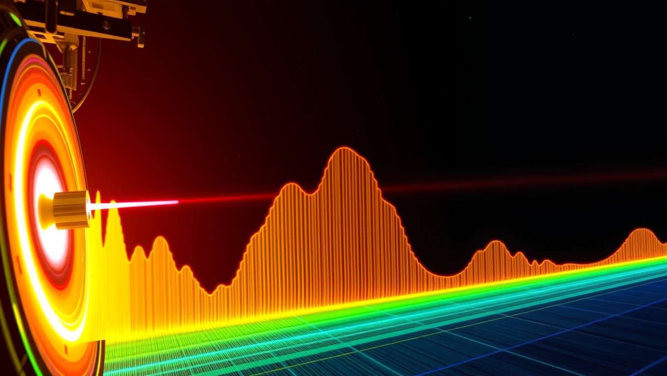
Neutrinos Get Even Lighter: The Latest Breakthrough in Astroparticle Physics
New data establish an upper limit of 0.45 eV/c2 (equivalent to 8 x 10-37 kilograms) for the neutrino mass. KATRIN measures neutrino mass in the laboratory using a model-independent method.


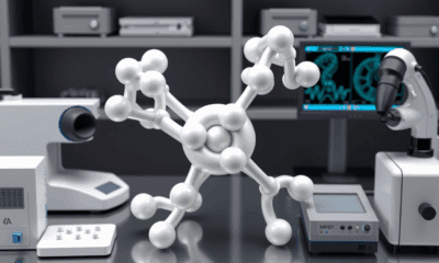

Batteries
“Reviving ‘Dead’ Batteries: The Path to a Greener Future”
Lithium battery recycling offers a powerful solution to rising demand, with discarded batteries still holding most of their valuable materials. Compared to mining, recycling slashes emissions and resource use while unlocking major economic potential. Yet infrastructure, policy, and technology hurdles must still be overcome.

Aviation
“Revolutionizing Titanium Alloys: New 3D-Printed Material Cuts Costs by 29% While Boosting Strength”
A team of engineers at RMIT University has developed a groundbreaking 3D-printed titanium alloy that s stronger, more ductile, and nearly 30% cheaper to produce than the traditional standard. By replacing expensive vanadium with more accessible elements and rethinking how titanium alloys are designed, the team created a material with improved performance and more uniform microstructure key factors for aerospace and medical applications.

Batteries
“Revolutionizing Energy Storage: AI-Driven Discovery of New Materials for Multivalent-Ion Batteries”
AI is helping scientists crack the code on next-gen batteries that could replace lithium-ion tech. By discovering novel porous materials, researchers may have paved the way for more powerful and sustainable energy storage using abundant elements like magnesium.


A New Horizon for Vision: How Gold Nanoparticles May Restore People’s Sight

Retiring Abroad Can Be Lonely Business

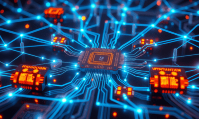
Revolutionizing Quantum Communication: Direct Connections Between Multiple Processors
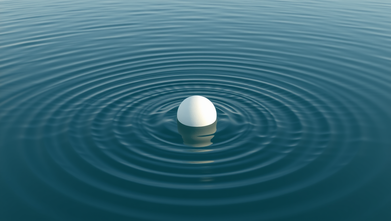
Harnessing Water Waves: A Breakthrough in Controlling Floating Objects

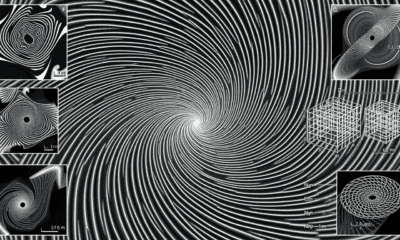
“Unveiling Hidden Patterns: A New Twist on Interference Phenomena”

Household Electricity Three Times More Expensive Than Upcoming ‘Eco-Friendly’ Aviation E-Fuels, Study Reveals
Reducing Falls Among Elderly Women with Polypharmacy through Exercise Intervention
-
 Detectors12 months ago
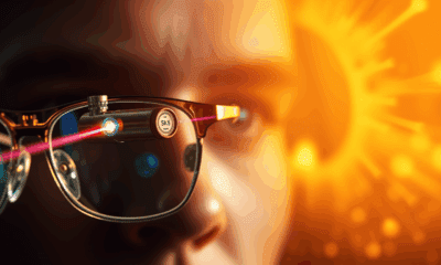
A New Horizon for Vision: How Gold Nanoparticles May Restore People’s Sight
-
Earth & Climate1 year ago
Retiring Abroad Can Be Lonely Business
-
Cancer1 year ago
Revolutionizing Quantum Communication: Direct Connections Between Multiple Processors
-
Albert Einstein1 year ago
Harnessing Water Waves: A Breakthrough in Controlling Floating Objects
-
Chemistry1 year ago
“Unveiling Hidden Patterns: A New Twist on Interference Phenomena”
-
Earth & Climate1 year ago
Household Electricity Three Times More Expensive Than Upcoming ‘Eco-Friendly’ Aviation E-Fuels, Study Reveals
-
Diseases and Conditions1 year ago
Reducing Falls Among Elderly Women with Polypharmacy through Exercise Intervention
-
Agriculture and Food1 year ago
“A Sustainable Solution: Researchers Create Hybrid Cheese with 25% Pea Protein”