While we try to keep things accurate, this content is part of an ongoing experiment and may not always be reliable.
Please double-check important details — we’re not responsible for how the information is used.
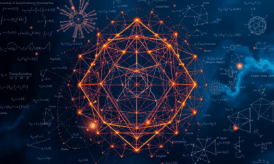
Detectors
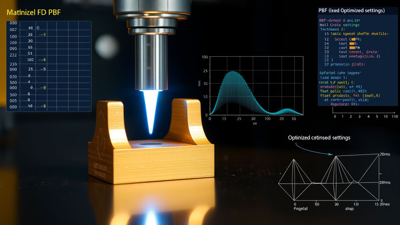
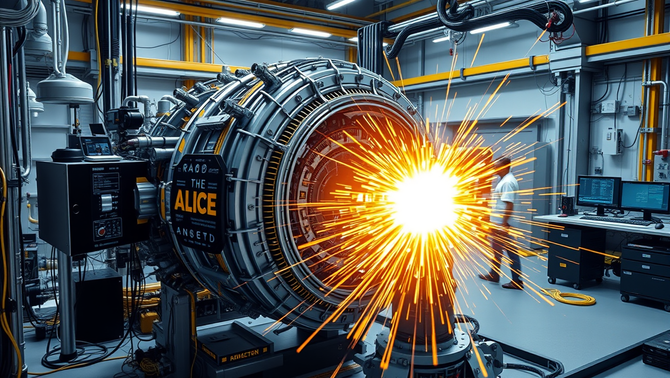
Revolutionizing Industrial Laser Processes with Machine Learning
Laser-based metal processing enables the automated and precise production of complex components, whether for the automotive industry or for medicine. However, conventional methods require time- and resource-consuming preparations. Researchers are now using machine learning to make laser processes more precise, more cost-effective and more efficient.


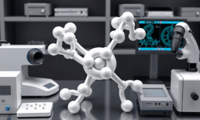

Chemistry
Scientists Stunned by Record-Breaking, Watermelon-Shaped Nucleus: Breakthrough Discovery in Nuclear Physics
Scientists in Finland have measured the heaviest known nucleus to undergo proton emission, discovering the rare isotope 188-astatine. It exhibits a unique shape and may reveal a new kind of nuclear interaction.

Chemistry
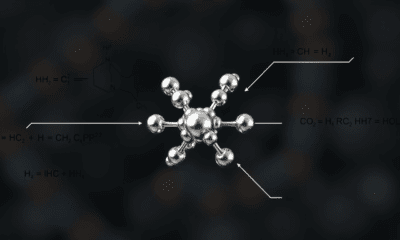
From Lead to Gold in a Fraction of a Second at the Large Hadron Collider
At the Large Hadron Collider, scientists from the University of Kansas achieved a fleeting form of modern-day alchemy — turning lead into gold for just a fraction of a second. Using ultra-peripheral collisions, where ions nearly miss but interact through powerful photon exchanges, they managed to knock protons out of nuclei, creating new, short-lived elements. This breakthrough not only grabbed global attention but could help design safer, more advanced particle accelerators of the future.
Cosmic Rays
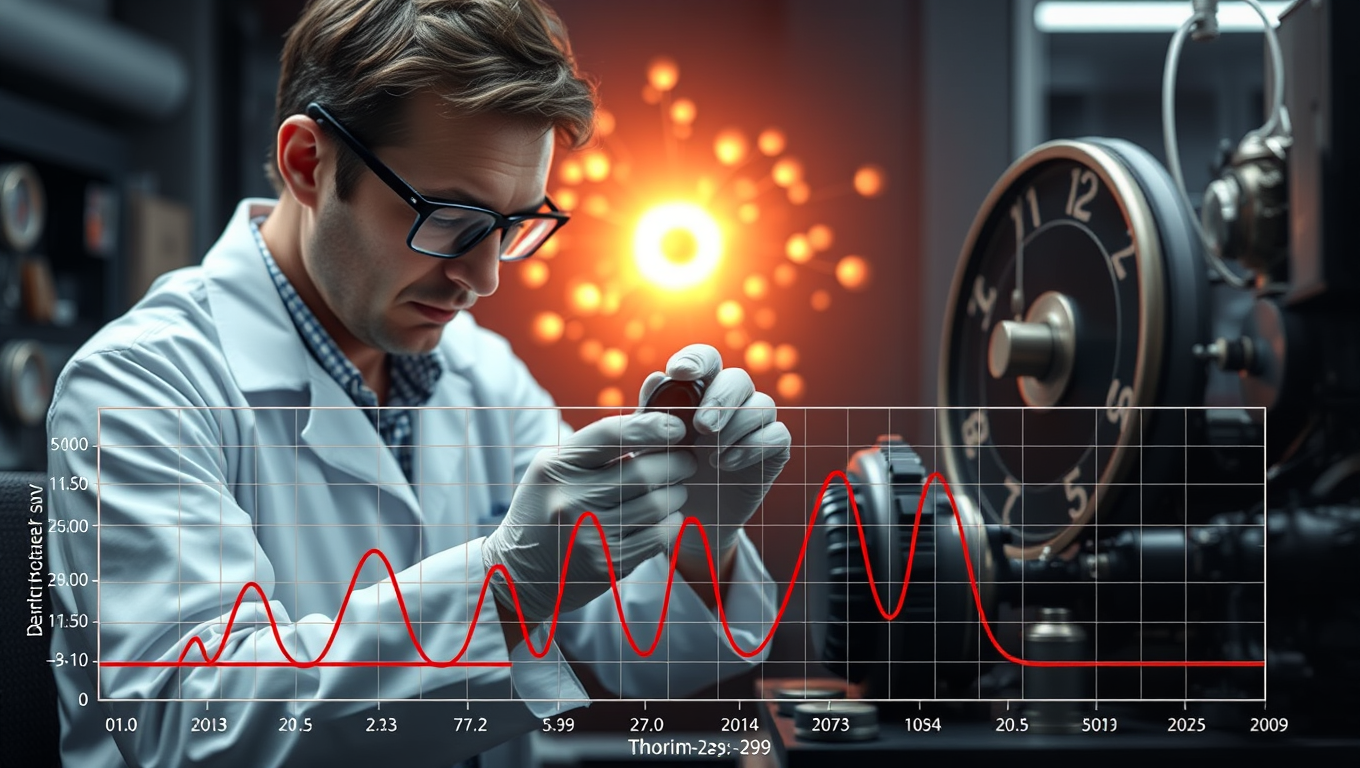
The Nuclear Clock That Could Unmask Dark Matter
Physicists are exploring thorium-229’s unique properties to create a nuclear clock so precise it could detect the faintest hints of dark matter. Recent measurement advances may allow scientists to spot tiny shifts in the element’s resonance spectrum, potentially revealing the nature of this mysterious substance.

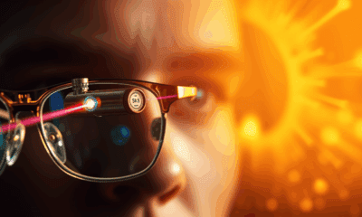
A New Horizon for Vision: How Gold Nanoparticles May Restore People’s Sight

Retiring Abroad Can Be Lonely Business

Revolutionizing Quantum Communication: Direct Connections Between Multiple Processors
Harnessing Water Waves: A Breakthrough in Controlling Floating Objects

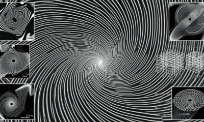
“Unveiling Hidden Patterns: A New Twist on Interference Phenomena”

Household Electricity Three Times More Expensive Than Upcoming ‘Eco-Friendly’ Aviation E-Fuels, Study Reveals
Reducing Falls Among Elderly Women with Polypharmacy through Exercise Intervention
-
 Detectors11 months ago
A New Horizon for Vision: How Gold Nanoparticles May Restore People’s Sight
-
Earth & Climate1 year ago
Retiring Abroad Can Be Lonely Business
-
Cancer12 months ago
Revolutionizing Quantum Communication: Direct Connections Between Multiple Processors
-
Albert Einstein1 year ago
Harnessing Water Waves: A Breakthrough in Controlling Floating Objects
-
Chemistry12 months ago
“Unveiling Hidden Patterns: A New Twist on Interference Phenomena”
-
Earth & Climate12 months ago
Household Electricity Three Times More Expensive Than Upcoming ‘Eco-Friendly’ Aviation E-Fuels, Study Reveals
-
Diseases and Conditions1 year ago
Reducing Falls Among Elderly Women with Polypharmacy through Exercise Intervention
-
Agriculture and Food12 months ago
“A Sustainable Solution: Researchers Create Hybrid Cheese with 25% Pea Protein”