While we try to keep things accurate, this content is part of an ongoing experiment and may not always be reliable.
Please double-check important details — we’re not responsible for how the information is used.
Computer Graphics
Unlocking Next-Generation Particle Physics Experiments with Quantum Sensors
Researchers have developed a novel high-energy particle detection instrumentation approach that leverages the power of quantum sensors — devices capable of precisely detecting single particles.


Computer Graphics
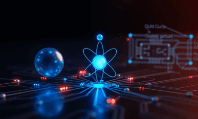
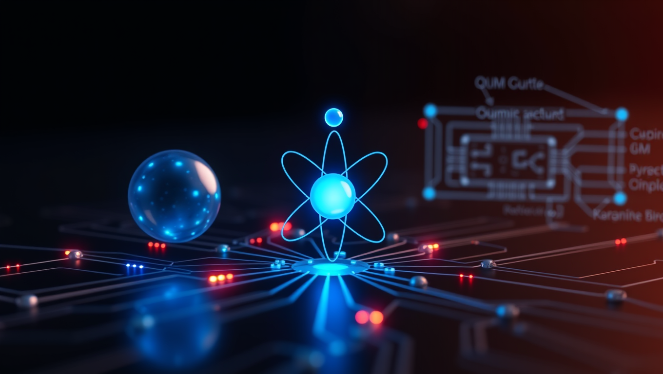
Cracking the Code: Scientists Breakthrough in Quantum Computing with a Single Atom
A research team has created a quantum logic gate that uses fewer qubits by encoding them with the powerful GKP error-correction code. By entangling quantum vibrations inside a single atom, they achieved a milestone that could transform how quantum computers scale.
Computer Graphics
The Quiet Threat to Trust: How Overreliance on AI Emails Can Harm Workplace Relationships
AI is now a routine part of workplace communication, with most professionals using tools like ChatGPT and Gemini. A study of over 1,000 professionals shows that while AI makes managers’ messages more polished, heavy reliance can damage trust. Employees tend to accept low-level AI help, such as grammar fixes, but become skeptical when supervisors use AI extensively, especially for personal or motivational messages. This “perception gap” can lead employees to question a manager’s sincerity, integrity, and leadership ability.

Child Development
Pain Relief Without Pills? VR Nature Scenes Activate Brain’s Healing Switch
Stepping into a virtual forest or waterfall scene through VR could be the future of pain management. A new study shows that immersive virtual nature dramatically reduces pain sensitivity almost as effectively as medication. Researchers at the University of Exeter found that the more present participants felt in these 360-degree nature experiences, the stronger the pain-relieving effects. Brain scans confirmed that immersive VR scenes activated pain-modulating pathways, revealing that our brains can be coaxed into suppressing pain by simply feeling like we re in nature.


A New Horizon for Vision: How Gold Nanoparticles May Restore People’s Sight

Revolutionizing Quantum Communication: Direct Connections Between Multiple Processors

Retiring Abroad Can Be Lonely Business
Harnessing Water Waves: A Breakthrough in Controlling Floating Objects

Household Electricity Three Times More Expensive Than Upcoming ‘Eco-Friendly’ Aviation E-Fuels, Study Reveals

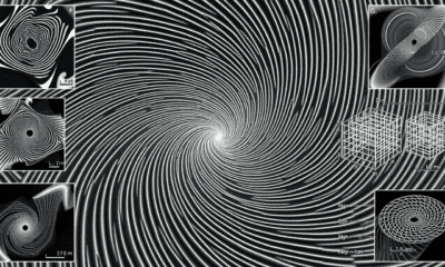
“Unveiling Hidden Patterns: A New Twist on Interference Phenomena”
Reducing Falls Among Elderly Women with Polypharmacy through Exercise Intervention
-
 Detectors1 year ago
A New Horizon for Vision: How Gold Nanoparticles May Restore People’s Sight
-
Cancer1 year ago
Revolutionizing Quantum Communication: Direct Connections Between Multiple Processors
-
Earth & Climate1 year ago
Retiring Abroad Can Be Lonely Business
-
Albert Einstein1 year ago
Harnessing Water Waves: A Breakthrough in Controlling Floating Objects
-
Earth & Climate1 year ago
Household Electricity Three Times More Expensive Than Upcoming ‘Eco-Friendly’ Aviation E-Fuels, Study Reveals
-
Chemistry1 year ago
“Unveiling Hidden Patterns: A New Twist on Interference Phenomena”
-
Diseases and Conditions1 year ago
Reducing Falls Among Elderly Women with Polypharmacy through Exercise Intervention
-
Agriculture and Food1 year ago
“A Sustainable Solution: Researchers Create Hybrid Cheese with 25% Pea Protein”