Connect with us
We’re experimenting with AI-generated content to help deliver information faster and more efficiently.
While we try to keep things accurate, this content is part of an ongoing experiment and may not always be reliable.
Please double-check important details — we’re not responsible for how the information is used.

Artificial Intelligence

Major Breakthroughs in Flat and Adjustable Optics: A New Era for Practical Applications

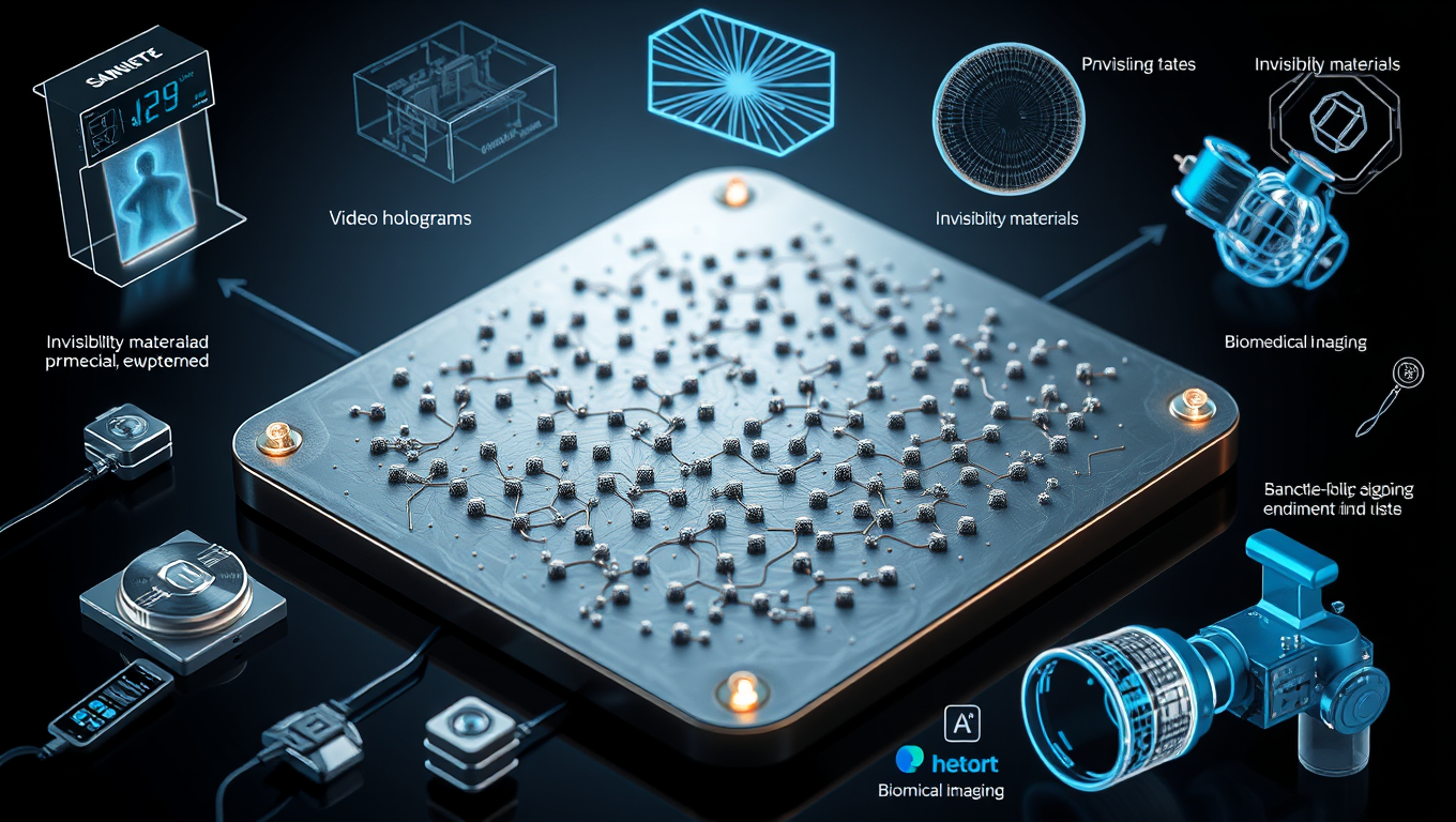
By carefully placing nanostructures on a flat surface, researchers have significantly improved the performance of so-called optical metasurfaces in conductive plastics. This is a major step for controllable flat optics, with future applications such as video holograms, invisibility materials, and sensors, as well as in biomedical imaging.
Avatar photo

Published

on

The researchers at Linköping University in Sweden have achieved a significant milestone in the development of controllable flat optics. By carefully placing nanostructures on a flat surface, they have improved the performance of optical metasurfaces made from conductive plastics. This breakthrough has far-reaching implications for various fields, including video holograms, invisibility materials, sensors, and biomedical imaging.

Traditional glass lenses are often curved to refract light in different ways. However, these lenses take up space and become impractical when miniaturized. Flat lenses, on the other hand, offer a promising alternative. They are made of metalenses, which form a rapidly growing field of research with great potential. Despite their limitations, metasurfaces have garnered significant attention due to their ability to control light using nanostructures placed in patterns on a flat surface.

“Metasurfaces work by placing nanostructures in patterns on a flat surface and becoming receivers for light,” explains Magnus Jonsson, professor of applied physics at Linköping University. “Each receiver captures the light in a certain way, allowing the light to be controlled as desired.”

However, one major challenge facing metasurface technology is the inability to adjust their function after manufacture. Researchers and industry have requested features such as turning metasurfaces on and off or dynamically changing the focal point of a metalens.

In 2019, Magnus Jonsson’s research group at the Laboratory of Organic Electronics showed that conductive plastics can crack this nut. They demonstrated that the plastic could function optically as a metal and be used as a material for antennas building a metasurface. The ability to oxidize and reduce allowed the nanoantennas to be switched on and off.

The same research team has now improved performance up to tenfold by precisely controlling the distance between the antennas, which helps each other through collective lattice resonance. This advancement enables conductive polymer-based metasurfaces to provide sufficiently high performance for practical applications.

While the researchers have successfully manufactured controllable antennas from conducting polymers for infrared light, their next step is to develop the material to be functional in the visible light spectrum as well.

This breakthrough has significant implications for various fields and opens up new possibilities for innovation. As research continues to push the boundaries of metasurface technology, we can expect to see exciting developments in video holograms, invisibility materials, sensors, and biomedical imaging equipment.

Artificial Intelligence

Breaking Through Light Speed: Harnessing Glass Fibers for Next-Generation Computing

Imagine supercomputers that think with light instead of electricity. That s the breakthrough two European research teams have made, demonstrating how intense laser pulses through ultra-thin glass fibers can perform AI-like computations thousands of times faster than traditional electronics. Their system doesn t just break speed records it achieves near state-of-the-art results in tasks like image recognition, all in under a trillionth of a second.

Avatar photo

Published

on

By

Imagine a world where computers can process information at incredible velocities, far surpassing today’s electronic systems. A groundbreaking study has made significant strides in achieving this vision by utilizing glass fibers to perform tasks faster and more efficiently. This novel approach involves harnessing the power of light to mimic artificial intelligence (AI) processes, leveraging nonlinear interactions between intense laser pulses and thin glass fibers.

The research collaboration between postdoctoral researchers Dr. Mathilde Hary from Tampere University in Finland and Dr. Andrei Ermolaev from the Université Marie et Louis Pasteur in France has successfully demonstrated a particular class of computing architecture known as an Extreme Learning Machine (ELM), inspired by neural networks.

Unlike traditional electronics, which approach their limits in terms of bandwidth, data throughput, and power consumption, optical fibers can transform input signals at speeds thousands of times faster. By confining light within glass fibers to areas smaller than a fraction of human hair, the researchers have achieved remarkable results.

Their study has used femtosecond laser pulses (a billion times shorter than a camera flash) to encode information into the fiber. This approach not only classifies handwritten digits with an accuracy rate of over 91% but also does so in under one picosecond – a feat rivaling state-of-the-art digital methods.

What’s remarkable about this achievement is that the best results didn’t occur at maximum levels of nonlinear interaction or complexity, but rather from a delicate balance between fiber length, dispersion, and power levels. According to Dr. Hary, “Performance is not simply a matter of pushing more power through the fiber; it depends on how precisely the light is initially structured, in other words, how information is encoded, and how it interacts with the fiber properties.”

This groundbreaking research has opened doors to new ways of computing while exploring routes towards more efficient architectures. By harnessing the potential of light, scientists can pave the way for ultra-fast computers that not only process information at incredible velocities but also reduce energy consumption.

The collaboration between Tampere University and Université Marie et Louis Pasteur is a testament to the power of interdisciplinary research in advancing optical nonlinearity through AI and photonics. This work demonstrates how fundamental research in nonlinear fiber optics can drive new approaches to computation, merging physics and machine learning to open new paths toward ultrafast and energy-efficient AI hardware.

As researchers continue to explore this innovative technology, potential applications range from real-time signal processing to environmental monitoring and high-speed AI inference. With funding from the Research Council of Finland, the French National Research Agency, and the European Research Council, this project is poised to revolutionize the computing landscape and unlock new possibilities for humanity.

Continue Reading

Artificial Intelligence

“Unlocking Sustainable Cement: AI-Powered Recipes for a Greener Future”

AI researchers in Switzerland have found a way to dramatically cut cement s carbon footprint by redesigning its recipe. Their system simulates thousands of ingredient combinations, pinpointing those that keep cement strong while emitting far less CO2 all in seconds.

Avatar photo

Published

on

The cement industry produces around eight percent of global CO2 emissions – more than the entire aviation sector worldwide. Researchers at the Paul Scherrer Institute PSI have developed an AI-based model that helps to accelerate the discovery of new cement formulations that could yield the same material quality with a better carbon footprint.

The rotary kilns in cement plants are heated to a scorching 1,400 degrees Celsius to burn ground limestone down to clinker, the raw material for ready-to-use cement. Unsurprisingly, such temperatures typically can’t be achieved with electricity alone. They are the result of energy-intensive combustion processes that emit large amounts of carbon dioxide (CO2). What may be surprising, however, is that the combustion process accounts for less than half of these emissions, far less. The majority is contained in the raw materials needed to produce clinker and cement: CO2 that is chemically bound in the limestone is released during the production process.

To address this issue, researchers at PSI have developed an AI-powered tool that can identify optimal cement formulations with lower CO2 emissions and higher material quality. This tool uses a combination of machine learning algorithms and genetic programming to search for the best recipe based on user-defined specifications.

The study was conducted as part of the SCENE project, an interdisciplinary research program aimed at reducing greenhouse gas emissions in industry and energy supply. The researchers involved came from various disciplines, including cement chemistry, thermodynamics, and AI specialization.

The results show that the AI-powered tool can identify promising formulations with real potential for reducing CO2 emissions and improving material quality. However, further testing is required to confirm these findings and ensure practical feasibility in production.

Some of the key takeaways from this study include:

* The cement industry produces around 8% of global CO2 emissions.
* The majority of these emissions come from raw materials rather than combustion processes.
* An AI-powered tool can identify optimal cement formulations with lower CO2 emissions and higher material quality.
* Interdisciplinary collaboration is essential for developing effective solutions to complex problems like this one.

Overall, the study highlights the potential of AI-powered tools in addressing sustainability challenges and improving material quality. As the demand for more sustainable materials continues to grow, researchers and industry professionals will likely continue to explore innovative solutions like this one.

Continue Reading

Artificial Intelligence

Rebooting US Chip Powerhouses: Sandia and CHIPS Act Join Forces for Semiconductor Supremacy

Once a global leader in chipmaking, the U.S. now lags behind. Sandia National Laboratories is spearheading a strategic comeback by joining a powerful new coalition the National Semiconductor Technology Center. Through cutting-edge research, collaborative partnerships, and workforce development, Sandia is aiming to reclaim semiconductor dominance, safeguard national security, and revolutionize tech innovation for everything from self-driving cars to AI processors.

Avatar photo

Published

on

By

Sandia National Laboratories has taken a significant step towards rebooting the United States’ semiconductor industry, joining the U.S. National Semiconductor Technology Center (NSTC) under the CHIPS and Science Act. This partnership aims to accelerate innovation, strengthen national security capabilities, and foster the development of cutting-edge technologies that will position the US as a global leader in chip production.

The US was once a powerhouse in semiconductor manufacturing, producing over 35% of the world’s chips in the 1990s. However, this share has since dropped to just 12%, with the country now relying on other nations for advanced chips used in smartphones, self-driving cars, quantum computers, and artificial intelligence-powered devices.

Sandia hopes to change that by leveraging its research and development partnerships, as well as its advanced cleanrooms and facilities, such as MESA. The lab’s senior manager of Technology Partnerships and Business Development, Mary Monson, emphasized the importance of collaboration, stating, “The CHIPS Act has brought the band back together… By including the national labs, U.S. companies, and academia, it’s really a force multiplier.”

Sandia’s role in the NSTC partnership is multifaceted. The lab will provide access to its facilities for other members, fostering collaboration and partnerships. Tech transfer is a core part of Sandia’s missions, and this initiative will build on that by helping private partners increase their stake in the industry while enabling Sandia to bolster its own mission.

The urgency of this effort is evident, as seen during the pandemic when car manufacturers were left idle due to chip shortages. An average car contains 1,400 chips, and electric vehicles use more than 3,000. Other nations are investing heavily in semiconductor manufacturing, with over $300 billion being poured into this sector.

Sandia’s senior scientist for semiconductor technology strategy, Rick McCormick, noted that the US CHIPS Act is a response to this global investment, aiming for the US to have more than 25% of the global capacity for state-of-the-art chips by 2032.

To achieve this goal, Sandia will focus on developing new technologies, training the workforce of the future, and expanding access to small companies and national security applications. The lab’s resources and partnerships can help create a ecosystem for packaging assemblies of chiplets, which communicate at low energy and high speed as if they were a large expensive chip.

In conclusion, Sandia National Laboratories’ partnership with the U.S. National Semiconductor Technology Center under the CHIPS and Science Act marks an exciting new chapter in the US semiconductor industry. By joining forces with other partners, Sandia aims to reboot the country’s chip powerhouses, strengthen national security capabilities, and position the US as a global leader in cutting-edge technologies.

Continue Reading

Trending